

CAC940J005
Product Description Features
• Customized 940nm Vertical-Cavity Surface-Emitting Laser
• Very low wavelength-temperature sensitivity
• Chip on submount or heatsink is available upon request
• Other wavelengths, chip dimensions, and emitter patterns are available uponrequest
Typical Applications
• 3D sensing.
Electro-Optical Characteristics
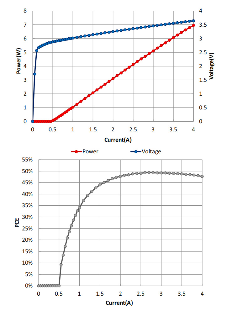
Parameters | Symbol | Min | Typical | Max | Units | Test Condition |
|---|---|---|---|---|---|---|
Optical Output Power | POP | 4.3 | 4.8 | – | W | Pulse 2.8A, 50℃ |
Threshold Current | Ith | – | 0.5 | 0.7 | A | Pulse 50℃ |
Operating Current | Iop | – | 2.8 | – | A | Pulse 2.8A, 50℃ |
Differential resistance | Rs | – | 0.21 | – | Ω | Pulse 2.8A, 50℃ |
Operating Voltage | Vop | 3.0 | 3.4 | 3.8 | V | Pulse 2.8A, 50℃ |
Slo pe Efficiency | ηs | 1.60 | 1.90 | – | W/A | Pulse 2.8A, 50℃ |
Power Conversion Efficiency | PCE | 42 | 49 | – | % | Pulse 2.8A, 50℃ |
Wavelength | λpeak | 934 | 940 | 946 | nm | Pulse 2.8A, 50℃ |
Spectral Width (RMS) | Δλ | – | 1 | 2.5 | nm | Pulse 2.8A, 50℃ |
Beam Full Divergence (D86) | ϕ | 20 | 24 | 28 | ° | Pulse 2.8A, 50℃ |
Wavelength coefficient | dλ/dT | – | 0.07 | – | nm/°C | Pulse 2.8A |
* All tests are under pulse condition on 1000Hz, 10%D.C. with heatsink temperature 50℃, unless otherwise specified.
Typical Performance Curves at 50°C
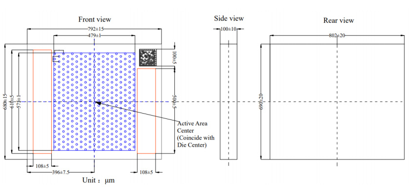
Mechanical Characteristics
| Parameter | Ratings | Units |
|---|---|---|
| Number of emitters | 361 | # |
| Emitter pitch (x) | 52 | µm |
| Emitter pitch (y) | 30.5 | µm |
| Chip Width | 792±15(Front); 802±20(Rear) | µm |
| Chip Length | 680±15(Front); 690±20(Rear); | µm |
| Chip Height | 100±10 | µm |
| Anode Contact | Emission side, Au surface | / |
| Anode bonding pad | 108 X610, 108 X500 | µm x µm |
| Cathode Contact | Backside, Au surface | / |
Chip dimension layout
Absolute Maximum Ratings
| Parameter | Conditions | Units |
|---|---|---|
| Operating Temperature | 0 to 85 | °C |
| Storage Temperature | -40 to 105 | °C |
Stresses beyond the parameters listed under Absolute Maxim Ratings may cause permanent damage to the chips.
Shipping Instruction
The unmounted chips are shipped on adhesive blue tape rings or Gel-Pak boxes.
Note: No responsibility is assumed for the use of these products. The products canemit Class IV radiation and must be operated with extreme care. Avoid directly viewingthe laser beam or exposure to specular reflections. Proper eye-wear must be worn at all times when operating. VCSEL Chips are electrostatic-sensitive device and proper ESD protection is required for handling.
