About Us
Vertilite Co., Ltd. (“Vertilite”) was founded in 2015 and has been offering vertical-cavity surface-emitting laser (VCSEL)chips and related modules of leading performance, as well as comprehensive technical support and services. Vertilite is dedicated to being the most reliable business partner of global customers. Vertilite products have now been widely deployed in the fields of consumer electronics,automotive electronics and optical communication.
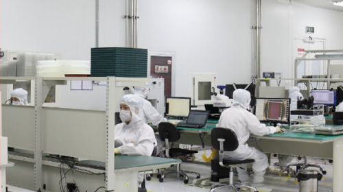
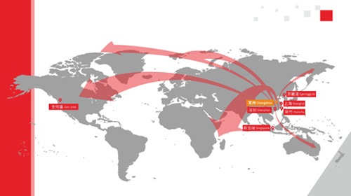
Vertilite, headquartered in Changzhou, has several subsidiaries in Shanghai, Shenzhen, Taiwan, Gyeonggi- do,San Jose and Singapore, aiming to provide services for local customers. The Changzhou facility houses state-of-the-art MOCVD epitaxial technology for 6-inch GaAs wafer growth as well as comprehensive backend packaging, testing, and qualification capability for bare VCSEL chips and related modules. The MOCVD line enhances Vertilite's capability of cutting-edge VCSEL technology and enables manufacturing competitiveness as well as supply sustainability. Vertilite is able to mass-produce products for customers in fields of consumer electronics, automotive electronics,optical communication and HBT epitaxy. Over 250 million VCSELs have been shipped out by the end of June, 2024, and no field failure is reported. Customized designs and engineering solutions are readily available to meet customers' diverse technical specifications.

- Journey
2015
"Shanghai Vertilite Optoelectronics" founded.
- Journey
2018
Changed to"Vertilite Co., Ltd.”
Entered Tier 1 Android smartphone supply chain.
- Journey
2019
6-inch epi production line built.
VCSEL chips shipment reaches 10 million.
- Journey
2021
Passed IATF 16949 certification.
Auto-grade DMS VCSELs shipped in volume.
- Journey
2022
Auto-grade VCSELs for IRillumation shipped in volume.
Auto-grade module lines built.
Auto-grade VCSELs for LiDAR shipped volume.
- Journey
2023
Mass production of AR-VCSEL for LiDAR.
HBT epi wafer qualified by foundry.
4x50G PAM4 VCSEL released.
- Journey
2024
2D VCSELs for solid-state LiDAR shipped in volume.
4x100G PAM4 VCSEL released.
3-inch Fab built
Vertilite was started by several Ph.D. graduates from Stanford University. Leading R&D and technology personnel graduated from Stanford, Duke, Yale, Tsinghua, Peking and Chinese Academy of Sciences and have extensive industrial experience in chip design, epitaxial growth, wafer processing and module packaging. Vertilite has successfully released multiple series of products with superior performance and shipped to customers.

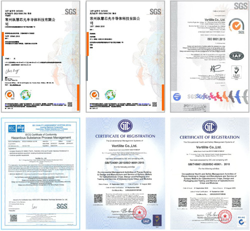
Vertilite obtained ISO14001Environmental Management System certification, ISO45001 Occupational Health and Safety Management System Certification and ISO9001Quality Management System and QC080000HazardousSubstance Process Management System Requirements, and IATF16949:2016. Vertilite has built a standardized, systematic, and professional operation system so as to offer superior products and services to customers.
Vertiltie has been awarded the"Potential Unicorn Enterprise in South Jiangsu National Innovation Demonstration Zone" for five consecutive years, and won the honorary titles of "Advanced New Technology Enterprise" and"Jiangsu Province Entrepreneurship and Innovation Unit" in 2020.In 2022, Vertilite won the title of "Jiangsu Province Specialized, High-End and Innovation-driven Enterprise"; Moreover, Vertilite has undertaken the construction of R&D platforms such as "Jiangsu High-end Laser Chip Engineering Technology Research Center", "JITRI- Vertical Joint Innovation Center", "National Engineering Research Center of Wide Band Gap Semiconductor-Changzhou Branch", and "Changzhou Optoelectronic Chip Key Laboratory".

Headquartered in Changzhou, Vertilite also operates offices in Shanghai in China, Silicon Valley in the USA, Seoul in Korea, Hsinchu in Taiwan, Kwun Tong in Hongkong and Singapore.

